
Printed Circuit Boards
Additively Manufactured PCBs
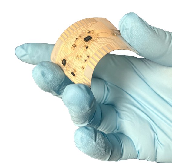
Additive manufacturing of printed circuit boards (PCBs) is transforming how electronics are designed and produced. Instead of relying on corrosive copper etching and plating methods, additive PCB manufacturing uses conductive inks to build circuits directly onto substrates—layer by layer. This approach, also called printed electronics, reduces waste, lowers costs, and shortens design-to-production timelines. With global demand for sustainable electronics, reshoring initiatives, and the need for supply chain resilience, additively manufactured PCBs are quickly becoming a disruptive alternative to traditional PCB fabrication.
The ACI Materials Solution
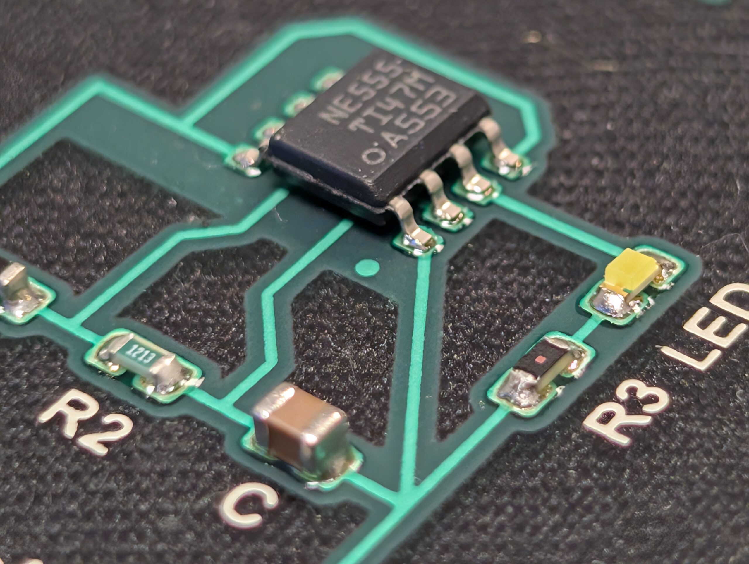
ACI Materials provides reliable solderable ink systems for additive PCB manufacturing. Our conductive silver inks allow surface mount devices to be directly soldered, producing durable, flexible, and high-performance circuits. By eliminating hazardous etching processes, ACI enables manufacturers to reduce costs, meet sustainability goals, and reshore PCB production back to North America and Europe.
Industry Applications
Our additively manufactured PCB technology can be used anywhere a one to four layer PCB is being used:
-
- Human Machine Interfaces
- Wearables
- Consumer Electronics
- Medical Devices
- Automotive
- Aerospace & Defense
- Sensors and Antennas
Benefits
- No etching or plating required
- Dramatically lower environmental impact during the manufacturing process
- Reduces production steps and enables reshoring
- Ease of prototyping using dispense equipment
- Can be used with a wide range of low-cost substrates
- Can be used for large area circuits (1-2M)
- Flexible and lightweight with robust mechanical properties
- Direct low-temperature solderability with standard PCBA equipment
What is Additive Manufacturing?
Additive manufacturing is a modern approach to circuit fabrication that builds electronics layer by layer instead of removing material through corrosive processes. In the context of PCBs, this is often referred to as printed electronics, where advanced conductive materials—like ACI’s silver ink—are deposited through high-speed printing methods rather than etched from copper-clad boards.
For PCB manufacturers and designers, this means:
Watch: How Printed Circuit Boards are Prototyped using ACI Materials
Our partners at Voltera demonstrate how printed circuit boards can be prototyped with our materials.
By using the same inks and substrates during prototyping, manufacturers can seamlessly transition to full-scale production with the same material set, demonstrated by our partners at FLEXOO.
Ready to Upgrade Your Materials?
ACI Materials is actively seeking partnerships with OEMs across a variety of industries to accelerate the adoption of additive PCB manufacturing. Our solderable conductive inks make it possible to replace traditional copper etching with a cleaner, faster, and more cost-effective process for one-to-four-layer board construction.